The size of the transistors inside semiconductor chips has nearly approached the diameter of human DNA molecules (2.5 nm), but manufacturers still want to shrink them further.
In 2009, the semiconductor industry started facing difficulties in shrinking chip sizes. Chiang Shang-yi, then TSMC’s director of research and development, thought he had a solution. Instead of cramming more transistors into an already tiny chip block, Shang-yi suggested to Morris Chang, TSMC’s founder, that the company should explore chip packaging – a process that was considered less advanced and gained little attention.
“I told Mr. Chang that the chip development process following Moore’s Law may slow down in coming years, so we should try something else to improve performance,” said Mr. Shang-yi.
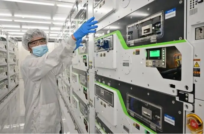
A worker in the cleanroom of an Intel factory in Indonesia.
Moore’s Law, established by Gordon Moore, Intel’s co-founder in 1965, states that the number of transistors on an integrated circuit will double every year, later amended to every 18 months. This finding also became the basis for another prediction: doubling the number of transistors equals doubling CPU performance on a similar cycle.
Previously, transistors were about a centimeter in size. After the above milestone, they were measured in millimeters. Today, they have reached the nanometer (nm) scale and are only equivalent to the diameter of human DNA.
Moore’s Law has shaped semiconductor industry development for many decades. Advances in the chip downsizing process catalyzed the entire industry from PCs, smartphones to the latest wave of AI processing chips. The race also caused companies like Taiwan’s TSMC, America’s Intel or Korea’s Samsung to spend billions of USD annually to produce chips with even smaller transistor sizes, pushing Moore’s Law towards its limits.
“If Moore’s Law really hits its ceiling, it would greatly affect the semiconductor industry,” said Shang-yi. “Without solutions, in 20 years the chip sector risks becoming a traditional rather than a high-tech industry like today.”
Catching up
There are signs that Shang-yi’s comments are becoming a reality. One of the biggest proofs is the narrowing gap between the leading company and chasing competitors.
“Running faster than the fastest runner is very difficult. But when the fastest can no longer run faster, those behind will catch up,” said Dan Hutcheson, Vice President of research firm TechInsights. “In a chip race, the leader cannot afford to stumble even once.”
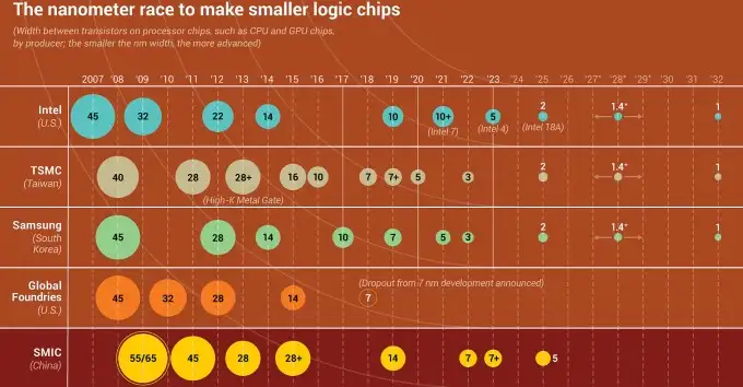
According to Nikkei Asia’s analysis, the technology gap between Intel and China’s SMIC is narrowing. Intel currently manufactures 5nm chips while SMIC already has 7nm chips. Experts attribute this partly to China’s determination towards semiconductor self-sufficiency, but it is also the result of the slowdown among flagships. Intel used to be at least 4 to 5 years ahead of its Chinese rival, equivalent to over two chip generations in manufacturing. Now, the gap is three years or 1.5 generations.
TSMC and Samsung currently manufacture 3nm chips while Intel is at 5nm. All three are racing to produce 2nm chips by 2025. By 2032, these three companies are expected to manufacture 1nm chips.

Nanometers technically refer to the transistor gate width on the chip. The smaller the gates allow cramming more transistors into the same area, making more powerful processors. But there is a minimum size limit—further gate shrinking will become impossible at some point. Hence, companies have to come up with innovations.
In the past, most chipmakers used a two-dimensional architecture. Intel was the first to move its transistors to a 3D structure called FinFET in 2012. TSMC and Samsung quickly followed suit.
Now, leading chip giants are targeting an even more complex transistor structure called Gate-all-around to increase chip power. The new structure is expensive but companies have to catch up.
In 2022, total capital expenditure by TSMC, Intel and Samsung Electronics exceeded 97 billion USD, twice as much as the amount the EU plans to spend to develop its chip sector in the next decade. “Costs are slowing everything down. In the past, TSMC would apply new technology every two years, now it’s three years and in the future it could be longer,” said Handel Jones, a veteran semiconductor expert and CEO of chip consulting firm International Business Strategies.
The slowing pace of Moore’s Law has presented companies like SMIC a “once-in-a-thousand-year” opportunity to narrow their gap with industry leaders. “Good opportunities are coming to Chinese businesses,” commented Wu Hanming from the Chinese Academy of Engineering.
Chip packaging – the new battlefield
TSMC started exploring chip downsizing alternatives through serious chip packaging from 2009. Chip packaging was initially seen merely as a way to protect integrated circuits. It didn’t require as advanced technology as chip manufacturing and didn’t deliver performance improvements like increasing transistor counts.
However, Shang-yi realized that connecting different chips, such as memory and processors, in new ways could lead to huge improvements. He convinced founder Chang to provide a 100 million USD budget and a 400-person team to realize the idea.
Success didn’t come instantly. “Some TSMC directors even laughed, saying my proposal had turned TSMC into a company that only runs 50 wafers per month,” recalled Shang-yi.
But now, chip packaging has become a new battlefield. This year, for the first time in 40 years, Intel had to redesign its chip architecture to take advantage of chip packaging.
Nvidia’s H100 GPU, the power behind ChatGPT, encapsulates the new trend. Its integrated design directly connects the graphics processor with six high-bandwidth memory chips using advanced packaging technology from TSMC.
In 2021, Intel and TSMC embarked on the largest chip packaging expansion plans with tens of billions of USD. Even the US government began noticing this field by allocating three billion USD for chip packaging research, along with the 52 billion USD semiconductor subsidy.
“We are in a race to stack all chips in a three-dimensional cake-like model, then package them into a single unit,” said Lars Reger, CTO of NXP Semiconductors.
Opportunities for China
“You don’t need too many advanced, complicated equipment for chip packaging, and you can also use packaging technology to advance the process from 7nm to 5nm and even 3nm,” said a director at Kinsus Interconnect Technology, a chip substrate supplier for Nvidia and AMD. “So in a way, the slowdown of Moore’s Law is a good point for Chinese chip manufacturers to narrow their gap with leading names.”
David Ma, President of semiconductor manufacturing system builder Nova Technology, argues that the burgeoning chip packaging sector will “provide China a shortcut opportunity.”
Chinese companies like SMIC and Huawei are undergoing their biggest expansion ever, having invested 24 billion USD in capital expenditure from 2020 to 2023. Despite limited capabilities, SMIC remains committed to achieving 5nm and even 3nm chip production goals with a dedicated R&D team led by co-CEO Liang Mong-Song, a veteran expert from TSMC and Samsung.
Meanwhile, Huawei has spent close to 81 billion USD on R&D since 2019 when it was added to the US entity list. In fact, Huawei’s HiSilicon had successfully designed 5nm chips and placed orders with TSMC before getting banned.
“Huawei has a proven track record of designing cutting-edge chips on par with Apple’s and Nvidia’s. The company is a key player behind China’s chip progress,” commented Brady Wang, a tech analyst at research firm Counterpoint Research.
Smaller Chinese chip companies are also emerging. In Jiangsu province, state-backed semiconductor packaging startup SJ Semiconductor is researching technology similar to TSMC’s. Another top chip assembly company Quliang Electronics in Quanzhou city plans to expand capacity at least four-fold over the next three years.
“China is accelerating its chip packaging capabilities,” revealed a semiconductor supply chain CEO. “They are tracking industry moves, despite not yet having mature packaging technology for mass utilization.”